Services
Drawing upon a team of specialists with a broad range of experience in image sensor design – SI Sensors is creating custom image sensor designs with cutting edge performance. In particular, the company’s in-house experts have specialist knowledge of visible and non-visible imaging technologies, optimised light detection and charge transfer, radiation-hard sensor design, and creating CCD-in-CMOS pixels to enable novel imaging techniques such as ultra-fast burst mode imaging.
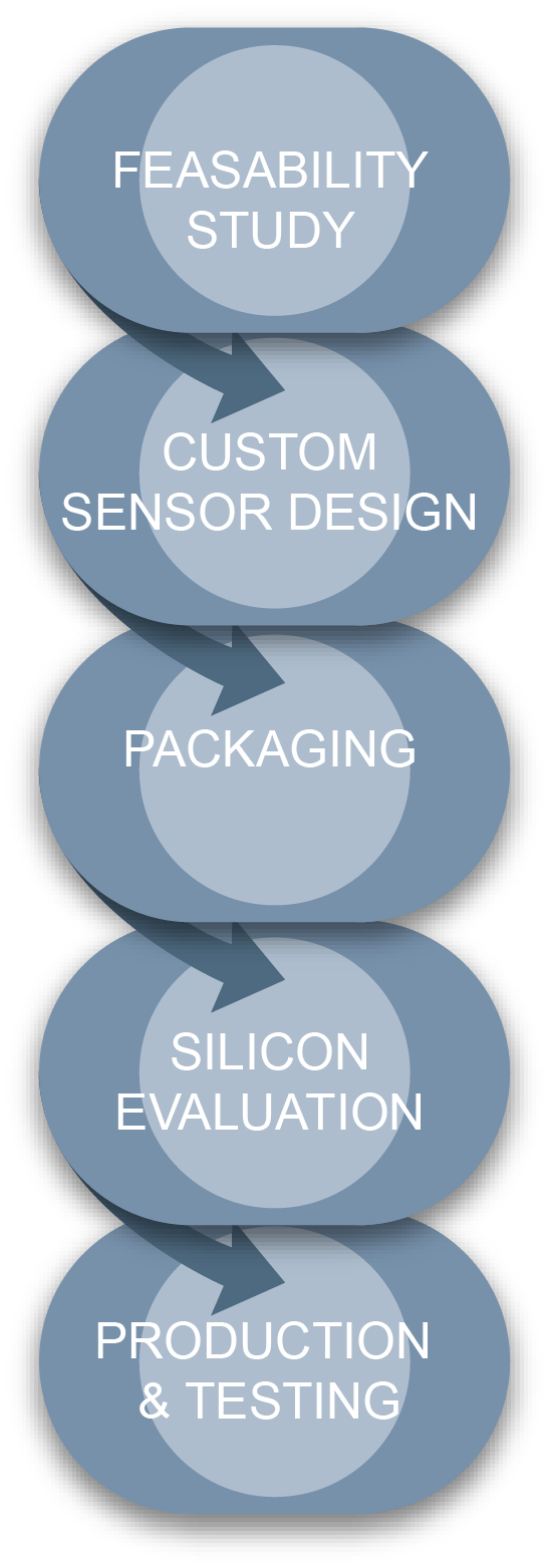
Feasability Study
A feasibility study will typically progress our design concepts to determine the optimal design and process option choices to achieve the required specifications of your sensor. It will review all critical aspects of the sensor design options and trade-offs including pixel design, analogue to digital conversion, digital data pipeline and data transmitter architectures as well as development of an initial product specification and an assessment of the risks. A cost/benefit analysis of the suitable manufacturing process options can be included to assist in the selection of an appropriate CMOS foundry and fabrication technology. It may also be appropriate to include an assessment of the packaging and test requirements of your sensor.
Custom Sensor Design
SI Sensors offer to perform all aspects of CMOS Image Sensor design consisting of:
• Circuit design
• Pixel optimisation
• Simulation
• Layout
• Verification
• Tape-out
Our capabilities include:
• Low noise CMOS design, to achieve the highest possible image quality
• Back side illumination, to improve image sensor quantum efficiency
• High dynamic range, to capture the most challenging scenes
• Global shutter, to minimize temporal artefacts in dynamic scenes
• CCD-in-CMOS pixels, to enable ultra-fast in-pixel storage
• Reticle stitching, to optimise sensor size
• Non visible imaging techniques, for near-infrared, UV, X-ray and charged particle imaging
• System-on-Chip sensor architectures, allowing for simplified camera system design and optimum performance
• We choose CMOS technologies between 180 nm and 65 nm process nodes, which typically offer the best compromise between image sensor performance and cost
Packaging
SI Sensors team have experience in developing bespoke image sensor packages for high reliability applications in harsh environments. We can accommodate challenging optical, mechanical, thermal and electrical interfaces and environmental conditions. Please contact us to discuss your requirements.
Silicon Evaluation
SI Sensors have in-house test facilities and engineering expertise. Characterisation is performed on all new image sensor designs with input signals and control timing optimised to maximise performance.
Production & Testing
SI Sensors can manage production from initial sample evaluation, through to mass production. We can develop and perform production screening testing to confirm specification compliance on batch samples or up to 100% of deliverable sensors. Our tests can be adapted to suit customer requirements and/or adhere to industry standards such as EMVA 1288 and ESCC 9020.
Request further infomation.

